In the current digital age where the word increasingly negotiates with a plethora of chipping in technologies, the Government of India has launched a major initiative to indigenously develop the semiconductor chip design competence on its journey towards an efficient, Atmanirbhar Bharat.
As part of the mission, the Ministry of Electronics and Information Technology (MeitY), has not only set up a dedicated development centre – ChipIN – under the aegis of C-DAC, and also collaborated with Seimens to impart the necessary skills to the country’s technology youth.
The takeaway for Indian AV from this major initiative is apparent. It is soon hoped to have not only a huge talent pool of chip designers but also an efficient infrastructure that can lead to indigenous manufacturing and herald a new era.
……………………………………………………………….
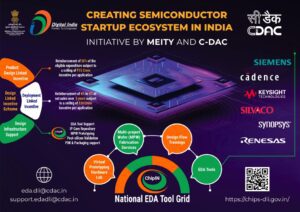
The Government of India is creating enabling environment for semiconductor chip design community with direct access to National Chip Design Infrastructure.
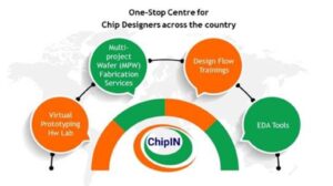
It has set up a dedicated development centre – ChipIN – in the Bengaluru facility of C-DAC (Centre for Development of Advanced Computing) for implementing the initiative as a one-stop access point for chip designers from across the country.

More, C-DAC is furthering its on-going initiative of training 20, 000 Indian engineering youth in chip design expertise by more than four times in the next five years- with collaborative support from German semiconductor major Seimens.
The objective is to empower as many as 85,000 technology engineering (B.Tech/M.Tech/PhD) professionals with necessary skills to design semiconductor chips and create a strong foundation for the semiconductor design community across India.

ChipIN Centre, one of the largest facilities established at C-DAC, offers an extensive range of semiconductor design workflows and solutions, striving to bring national chip design infrastructure directly to the semiconductor design community across the country. The centralized facility hosts most advanced tools for the entire chip design cycle- going up to 5 nm or still advanced node.
The facility also offers compute and hardware infrastructure, IP cores, and expertise to provide comprehensive services for design fabrication at the SCL foundry and packaging to academic institutions under C2S (Chips to Start-up) Programme and DLI (Design Linked Incentive) Scheme MeitY.
Charkha to Chips: Atmanirbhar Bharat

Presently engaged with an estimated number of 20,000+ students at 250+ academic institutions and entrepreneurs at 45 start-up projects, ChipIN Centre aims at providing access of state-of-the-art EDA (electronic design automation) tools to 85,000 students at B.Tech, M.Tech and PhD level to design semiconductor chips the coming five years to meet the objectives of Atmanirbhar Bharat.
(A list of institutions getting access of EDA Tools can be accessed at https://c2s.gov.in/EDA_Tool_Support.jsp
Considering the growing demand for EDA tools from Siemens amongst researchers and opportunity to scale the established infrastructure at ChipIN Centre, Siemens has extended the current usage scope of its EDA tools from 120 colleges to over 250 academic institutions under C2S programme, with its atest Veloce hardware-assisted verification solution.
Boost India’s Semiconductor Vision

“We were receiving the huge demand from students, researchers, faculty members and entrepreneurs across the country for further enhancing and extending the EDA, and other design solutions from Siemens,” said Sunita Verma, Group Coordinator (R&D in Electronics & IT), Ministry of Electronics and IT. “The enhanced support from Siemens at the ChipIN Centre will play a crucial role in fulfilling the vision of turning India into a semiconductor powerhouse.”
Empowering GenNext for a Self-Sustaining Semiconductor Ecosystem
“India today presents a significant opportunity for aspiring entrepreneurs and researchers to be at the forefront of designing and redefining the semiconductor systems, devices and products of the future,” said Ruchir Dixit, Vice-President and Country Manager (EDA), Siemens Digital Industries Software.

“Siemens is proud to extend its participation in the C2S Programme by expanding access of EDA technology solutions to 250 educational institutions across India,” Dixit said. “Our contribution is a testament of alignment with the nation’s unwavering commitment to building a robust and self-sustaianing semiconductor ecosystem,” he emphasized. “The initiative will go a long way to empower the next generation of engineers, researchers and entrepreneurs to drive India’s technological advancements and propel the nation towards becoming a global powerhouse.”


